
AMD EPYC Venice 256-Core CPU Signals a New Era of Zen 6c Density on TSMC 2nm
AMD's flagship EPYC Venice processor combines unprecedented core density with an advanced chiplet design built for AI infrastructure.
Hardware by Masaru Hoshino on Jul 29, 2026
AMD's next-gen EPYC Venice CPUs have already sparked massive enthusiasm. Still, a newly disclosed die rendering has now given the best look yet at what might become one of the most ambitious server processors ever created.
Banners advertising the keynote for Advancing AI 2026 at Moscone Center in San Francisco seem to have leaked the internal design of the flagship 256-core EPYC Venice processor, allowing hardware fans a peek at the company's next step forward in high-performance computing.
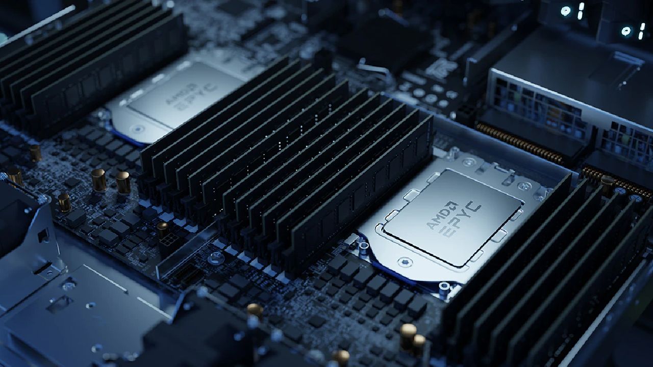
The image underscores months of anticipation surrounding Zen 6's aggressive scaling plan. AMD seems more focused on pushing computing density to the fullest with a very advanced chiplet design that allows for a huge increase in the number of threads, rather than just chasing a higher clock speed and a few more cores.
They are also taking advantage of the latest in semiconductor manufacturing technology. If the depiction is a good likeness of the final product, EPYC Venice looks to be one of the most advanced x86 CPUs ever designed.
Silicon Surgery: A Massive Chiplet Design Built for Extreme Compute
The leaked die architecture shows a massive package with eight computing chiplets (CCDs) around two giant core I/O dies, taking AMD's modular chiplet philosophy to new extremes beyond any previous EPYC generations.
Venice raises the computation density above previous EPYC processors that had fewer CPU cores per CCD, with 32 Zen 6c cores per CCD. The visualization reveals that each compute die has two 16-core Core Complexes (CCXs), creating a very orderly design that is both scalable and easy to manufacture. And that combination gets you a whopping 256 CPU cores and 512 simultaneous threads in a single processor package across all eight CCDs.
This degree of thread density is more than a number milestone. "Massive parallelism is more important than raw clock speed for modern AI inference, cloud virtualization, scientific simulations and hyperscale workloads. Doubling down on dense Zen 6c computing chiplets, AMD seems to be going for those enterprise environments where maximizing throughput per socket is more important than traditional desktop-style performance measurements.
The modular layout also showcases the ongoing growth of AMD's chiplet approach. This enables each component to be manufactured on the process technology that best suits its workload. This improves manufacturing yields and allows for significantly larger processor configurations than could be realistically achieved by conventional monolithic designs.
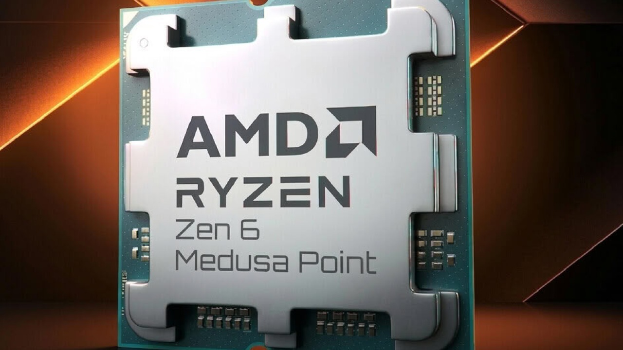
32 Zen 6c Cores Per CCD Push Thread Density to New Heights
The most important takeaway from the depiction is that each individual compute die consists of 32 Zen 6c cores. The number of CPU cores crammed onto a single CCD is a huge jump in computation density over prior versions of EPYC. With the Zen 6c, AMD can focus on efficiency and growing the number of cores without giving up on the performance that people expect from today's x86 server chips.
Each CCD seems to have two separate 16-core CCXs, which will give it a balanced interior, making it easier to arrange the cache and helping distribute work better across hundreds of threads running at the same time.
This architecture may greatly enhance VM density for cloud providers and hyperscale data centers, and can significantly cut down hardware needs at the rack level. Higher thread counts stuffed into fewer physical sockets are a big help for AI preprocessing, containerized services, database workloads, and virtualization platforms.
Instead of developing a bigger, monolithic silicon, AMD is doubling down on an approach that scales horizontally through chiplets. Venice is a demonstration of how far that mindset may go when combined with next-generation manufacturing technologies.
TSMC 2nm Brings a Historic Manufacturing Milestone
The architectural story is made even more stunning by Venice's production technique. With EPYC Venice, we look forward to the first HPC processor to reach volume production with TSMC's 2nm process technology, a historic milestone for the semiconductor industry.
This next-generation node also has gate-all-around (GAA) nanosheet transistors, replacing the long-standing FinFET design that has powered modern CPUs for years. In GAA technology, electrostatic regulation is much enhanced. This leads to transistors with lower leakage current and better performance and efficiency. In a 256-core CPU, these efficiency benefits are not just nice to have; they are a need.
But just packing hundreds of CPU cores onto one box will cause serious thermal and power delivery problems. Unless you make major improvements in transistor density and power efficiency. The transition to TSMC's 2nm node gives AMD more transistor budget while simultaneously helping manage power consumption across an extraordinarily large processor.
The increased density also provides room for larger caches, enhanced interconnects, improved memory subsystems, and more sophisticated AI acceleration capabilities without dramatically increasing package size.
Combined with AMD's mature chiplet approach, the 2nm transition could redefine what is practical for enterprise CPU scaling over the coming years.
Built for the AI Infrastructure Era
While EPYC Venice remains a general-purpose server processor, its specifications clearly reflect the changing priorities inside modern data centers.
Artificial intelligence workloads increasingly require enormous CPU resources for orchestration, preprocessing, storage management, networking, and feeding accelerators such as GPUs. Rather than competing directly with AI accelerators, processors like Venice serve as the central coordinators that keep massive GPU clusters operating efficiently.
With 512 simultaneous threads, Venice appears engineered for exactly these environments. Large language models, cloud-native applications, HPC simulations, virtualization clusters, and enterprise-scale databases all continue demanding higher thread counts, larger memory bandwidth, and better efficiency per rack. Venice seems positioned to address each of those priorities simultaneously.
The dual I/O die arrangement also suggests AMD continues investing heavily in scalable memory and connectivity infrastructure, ensuring the enormous core count can remain fed with sufficient data rather than becoming bottlenecked by system bandwidth.
Editor, NoobFeed
Gaming Hardware Updates
No Data.