
AMD's Zen 6, Zen 7, And Zen 8 Roadmap Explained Through 2030
AMD confirmed a CPU roadmap extending through 2030, covering Zen 6, Zen 7, and Zen 8 architectures.
Hardware by Nahe Yan on Jul 25, 2026
AMD has laid out an aggressive multi-generation roadmap for its Zen CPU architecture, confirming that major manufacturing leaps will now arrive back-to-back rather than every other generation. The plan extends well into the next decade and signals a shift in how quickly the company intends to advance its process technology.
AMD shared a new CPU roadmap that now extends through its Zen 8 family in 2030. Though this roadmap is built around server processors, we expect it to carry over to desktop parts as well, since AMD uses the same core complex across both segments. That shared chiplet design is the entire reason AMD can scale from lower-end consumer parts up to its highest-end server chips using the same underlying building blocks.
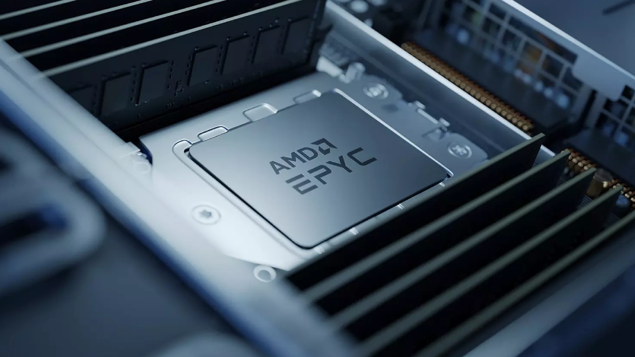
Zen 6 Marks a Major Leap to 2nm
AMD's upcoming Zen 6-based Venice processors are listed as the company's first CPUs to use 2nm technology. That represents a substantial jump forward, since the current Zen 5 compute dies are built on TSMC's 4nm process. In moving to Zen 6, AMD is effectively skipping past 3nm manufacturing entirely and going straight to TSMC's most advanced 2nm node.
Just two years later, AMD's roadmap lists its Zen 7-based Florence processors, which will include both standard Zen 7 and denser Zen 7c cores. AMD has stated that Florence will use a next-generation process node, confirming that Zen 7 will make another manufacturing jump immediately after Zen 6 moves to 2nm.
Because AMD relies on the same standard compute chiplet across its desktop and server lineups, this also confirms that desktop Zen 7 processors will move to that newer node alongside their server counterparts. AMD has not officially named the node, though a separate report from Taiwan's Commercial Times claims that AMD's Zen 7 compute die, codenamed Grimlock, will be manufactured using TSMC's A14 process.
Zen 7 Florence is scheduled for 2028, the same year TSMC expects A14 to enter production.
A14 represents a significant jump in TSMC's naming convention. The A stands for angstrom, with 14 angstroms converting to 1.4nm. That figure does not mean the transistors themselves contain a specific component measuring exactly 1.4nm, since modern process names have functioned mainly as marketing terms for some time rather than precise transistor measurements.
Even so, TSMC's shift from its traditional nanometer branding to angstrom branding still carries weight, signaling that the company views this as the start of a new era in semiconductor manufacturing. Technically, A14 sits two named process generations beyond the original N2 node, since TSMC also has an A16 node positioned in between.
We would not necessarily call that two complete traditional node shrinks, since A16 functions more as a specialized evolution of the 2nm family, adding backside power delivery. At the same time, TSMC describes A14 as the true full node advancement beyond N2. Regardless of how the naming breaks down, AMD appears committed to delivering major manufacturing leaps with every generation rather than spacing them out every other cycle.
Editor, NoobFeed
Gaming Hardware Updates
No Data.