
AMD Zen 6 Epyc Venice Specs and Pricing Revealed With 256 Cores
AMD's Zen 6 Venice CPUs Combine 2nm Technology, DDR5-12800 Support, and PCIe 6.0 Connectivity.
Hardware by Nahe Yan on Oct 01, 2026
AMD just revealed pricing and specs for its first Zen 6 CPUs, and they're insane. Specifically, we're talking about AMD's new EPYC 9006 server chips, code-named Venice. While we have seen some pretty wild benchmarks for these, AMD has now released the full lineup with specs and, more importantly, pricing.
As you can see, these CPUs range from 8 cores and 16 threads with the EPYC 916 to 256 cores and 512 threads with the EPYC 9996. That highest-end chip is technically AMD's dense Zen 6C chip, but even here, the specs are notable. To start, the base clock is 2.55GHz, which may not sound that great.
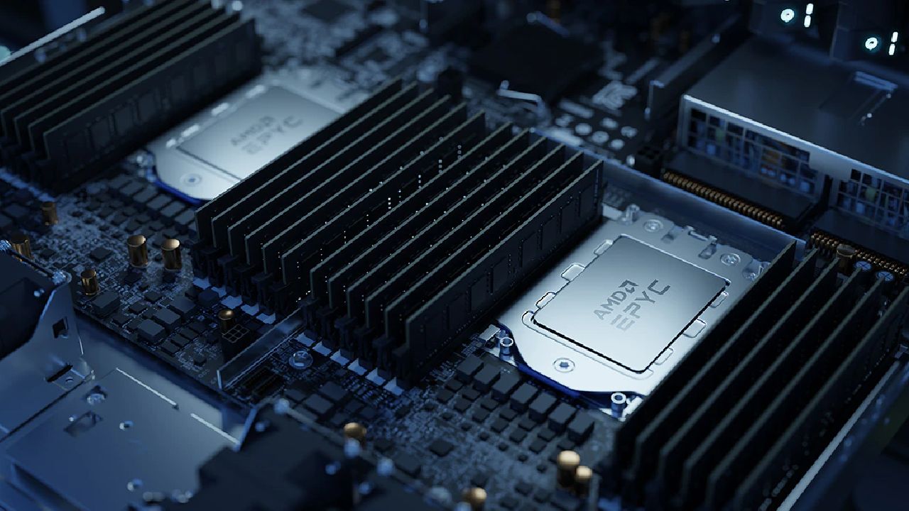
Zen 6 Venice Uses TSMC's 2nm Process
It also comes with 1,024MB of L3 cache and a 600W TDP. As for price, the 8-core CPU starts at $700 and goes up to $14,994 for the 256-core part. Obviously, $15,000 seems pretty insane. But we can't help but look back to around the time EPYC first launched in 2017, before Intel actually had competition.
Around this time, Intel released its Skylake Xeon Scalable chips, with its highest-end model, the Platinum 8180M, a 28-core, 56-thread CPU that cost around $13,000. Now, you might argue that this was many years ago, so things have obviously advanced since then. But you need to remember that this was 2017.
So the actual purchasing power of $13,000 was probably double what it is today. Inflation has been around 37% since then, but that includes things that haven't really gone up much and that we don't often buy. We've gone from 28 cores for $13,000 before today's inflation to 256 cores for $15,000 with today's inflation in less than a decade.
Moving back to the specs, don't forget all of this uses TSMC's 2nm process, with AMD as the first high-performance computing product to enter production on TSMC's new technology. The platform itself is also notable.
AMD's RX 10000 GPU Could Use a Large Compute Die
The highest-end chip supports 16 DDR5 channels, including MR DIMMs, running at up to 12,800 MT/s, delivering up to 1.6 TB/s of memory bandwidth, along with PCIe 6.0. Ultimately, though, this makes me increasingly excited to see what AMD does with Zen 6-based Ryzen.
AMD's RX 10000 looks set to be a large chip, and AMD itself appears to have provided more information through a new driver. As many of you know, we've talked about leaks claiming that AMD's next-gen gaming GPUs could go up to 154 CUs, a whopping 2.44 times as many cores as the 9070 XT.
That specific high-end card was reportedly set to be made from their AT0 GPU. And of course, the question becomes: how in the world is AMD going to fit that many cores on its chip? Originally, the well-known leaker Kepler L2 had a theory.
AMD's AT0 would split the shaders across four separate shader-engine dies.
Except that, not long after discussing this, Kepler found something in AMD's own Linux driver that seemingly killed that theory. A new AMD GPU patch adds support for Graphics Core 13; AMD literally defines the maximum number of AIDs and XCDs as 1 each.
So after finding it, Kepler immediately corrected himself, saying that AT0 instead appears to use a single AID and a single XCD. He later clarified that the configuration is one MID, one AID, and one XCD. The MID would handle things like multimedia and I/O, while the AID would include memory controllers and cache.
But the important part is that the XCD is the actual compute die containing the shaders. So, it's still technically a multi-chip module, but all those cores are apparently set to go on a single die. And if that rumored 154-CU configuration is real, AT0 could end up being one of the largest compute dies AMD has ever put into a gaming GPU.
Editor, NoobFeed
Gaming Hardware Updates
No Data.