
CXMT G5 DRAM Enters Mass Production With 24Gb LPDDR5X
CXMT’s G5 DRAM platform enters mass production with denser LPDDR5X memory and higher wafer-level die output.
Hardware by Nahe Yan on Oct 08, 2026
The memory industry continues to see changes in DRAM capacity, manufacturing, and production efficiency. CXMT has announced that its fifth-generation DRAM platform, G5, has entered mass production, with 24-gigabit LPDDR5X memory among its first products. The platform offers higher memory density and wafer-level production changes, but its real impact will depend on yield and production volume.
On September 20 at the World Manufacturing Convention in Hefei, CXMT announced that its fifth-generation DRAM platform, called G5, is now in mass production. The company is producing chips on production lines, not prototypes or lab samples. The first products built with the platform include a 24-gigabit LPDDR5X memory die.
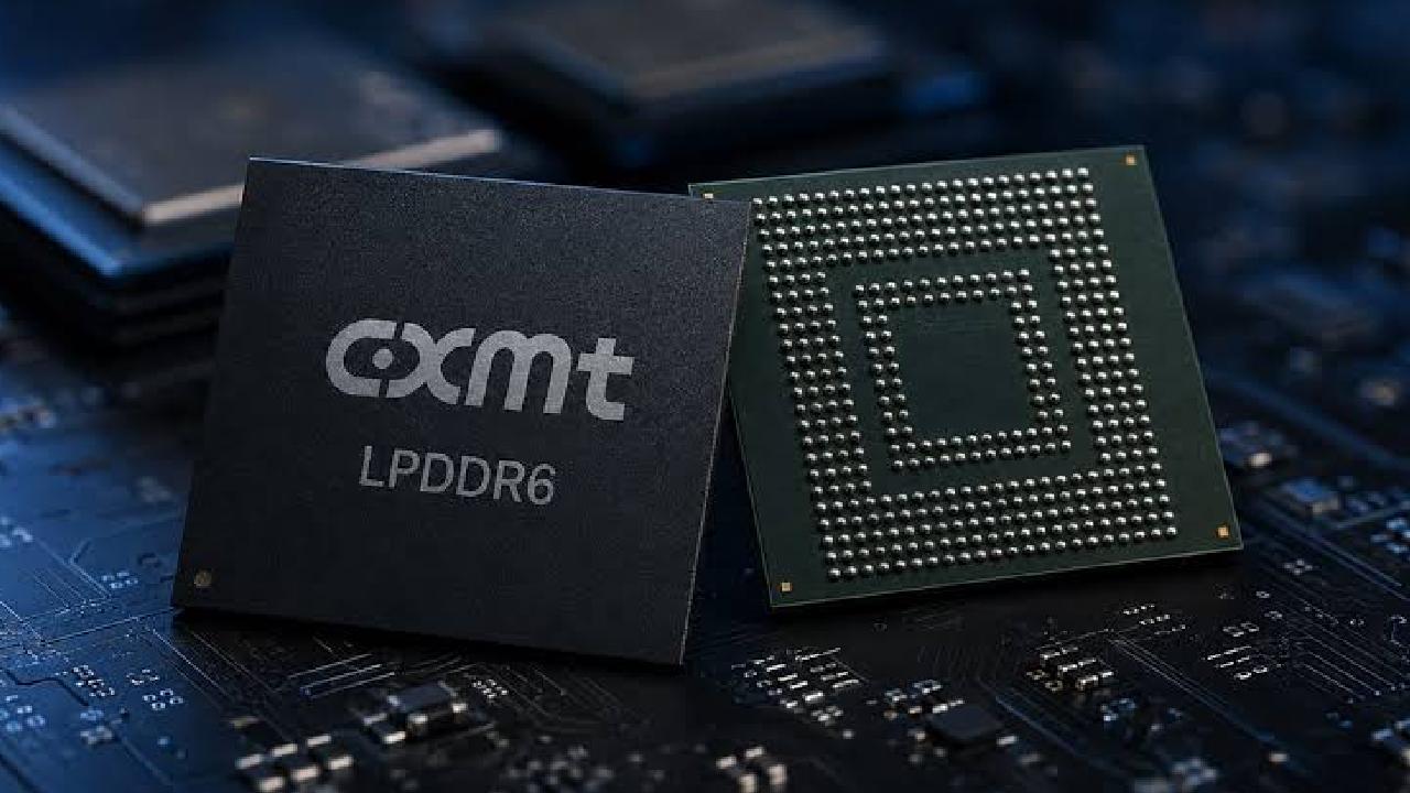
CXMT G5 Enters Mass Production With 24Gb LPDDR5X Dies
CXMT says G5 has entered mass production alongside two 24-gigabit LPDDR5X products. They come in 496-ball and 245-ball packages and target smartphones and portable electronics. According to the company, both products have already passed production line verification.
An important distinction also exists between gigabits and gigabytes. A 24-gigabit memory die provides roughly 3GB of capacity. CXMT's previous chips in this category reached 16gigabits, or 2GB. This means a single die has moved from 2GB to 3GB. A phone manufacturer that wants 24GB of RAM could therefore use eight of the new dies instead of 12 of the older dies.
That means fewer dies for the same capacity, or more capacity within the same space. CXMT Vice President Luo Shaodong, who heads the company's marketing center, also said the company's process capability now matches the most advanced nodes currently in mass production across the industry. That claim requires closer examination.
CXMT's announcement contains two separate claims involving a 50% increase, and they refer to different parts of the manufacturing process. The first is that the new die holds 50% more bits than the previous 16GB die. The second concerns production output: CXMT says G5 produces at least 50% more gross dies per wafer than its fourth-generation G4 platform.
The active area half pitch is one specific measurement within the memory array.
The array can be viewed as a grid of repeating lines, with the pitch representing the distance between adjacent lines. Half pitch is half that distance and indicates how tightly the memory cells' active regions are packed. An 11.95nm measurement is not a node name for the entire chip.
Samsung, SK Hynix, and Micron use DRAM generation labels such as 1B and 1C, and those labels do not map directly to one single physical dimension. Therefore, comparing CXMT's 11.95nm active area half pitch with a competitor's generation label does not provide a direct node-to-node comparison. The measurement also has no connection to the 3nm figures used for smartphone processors.
CXMT achieved the 11.95nm active area half pitch using self-aligned quadruple patterning, or SAQP. Instead of printing the smallest lines in a single lithography step, the process starts with a larger pattern, adds a thin film, and uses sidewall spacers as the new pattern. The process is repeated to increase line density.
Editor, NoobFeed
Gaming Hardware Updates
No Data.