
CXMT's New DRAM Technology Targets Higher Chip Capacity
CXMT's fifth-generation DRAM technology increases memory density and wafer productivity through manufacturing improvements and advanced patterning techniques.
Hardware by Shinji Okazaki on Oct 28, 2026
China's memory industry is advancing in DRAM manufacturing, raising questions about what engineers can achieve without access to the most advanced manufacturing tools. CXMT says its latest platform packs memory more densely and improves wafer productivity. Key details include its manufacturing process, memory capacity, and its ability to translate these developments into products that can compete in the market.
The biggest development is that CXMT says the platform is entering production. On September 20, 2026, the company announced its fifth-generation DRAM technology, called G5, at the World Manufacturing Convention in Hefei. That places the development beyond a laboratory demonstration.
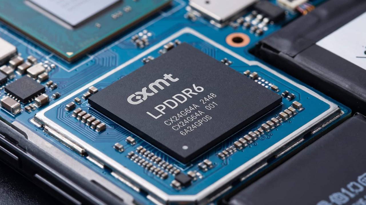
CXMT Announces Fifth-Generation DRAM Technology
Although the announcement alone doesn't show how smoothly factories are operating, the next question is what those factories are making. The headline measurement describes tighter spacing inside the memory array. CXMT reports an active area half-pitch of 11.95nm. Think of that as one measurement within a larger design.
It shows progress in packing structures together, but it doesn't tell the whole story on performance. Comparing manufacturers requires more than putting two small numbers side by side and declaring a winner. The clearest product connection comes from two new mobile memory chips. Both offer 24Gb per die, which CXMT says increases capacity by 50% compared with equivalent previous products.
Gigabits matter here. This is not a claim that each die contains 24GB. For device designers, greater capacity in individual components can create useful packaging options, linking manufacturing improvements to decisions about actual phones. CXMT reports at least 50% more gross dies per wafer, normalized to an 8Gb capacity baseline.
That qualification makes the comparison more meaningful because it controls for memory capacity. However, gross dies include chips before final acceptance testing. More potential chips therefore create an opportunity, but they do not automatically guarantee the same increase in saleable output. The capacitor result adds another dimension to the achievement.
The company reports a depth-to-width ratio of 45:1, describing slender storage structures.
Picture the challenge of building narrow shafts consistently across an array. Their shape matters because shrinking a memory cell still requires dependable electrical behavior. Density matters only when those structures work together. Together, these details turn a headline into a concrete manufacturing story. We have a reported production milestone, specific dimensions, and identifiable products.
The central technique is self-aligned quadruple patterning (SAQP). CXMT identifies it in the G5 announcement. Rather than relying on a single exposure to create the required spacing, this family of techniques adds deposition and etching steps to multiply pattern features. The precision comes from building a structure through a sequence of controlled steps, which brings the manufacturing process itself into focus.
This approach explains why existing lithography tools can remain valuable. ASML documents DUV systems designed to support double and multiple patterning for smaller manufacturing nodes. A machine's exposure resolution therefore does not, by itself, describe every structure a complete process can produce. The techniques matter.
Editor, NoobFeed
Gaming Hardware Updates
No Data.