
Intel Reveals DDR5 Engineering Challenges Behind 256GB CQDIMMs
Intel exposes the engineering challenges behind unreliable DDR5 prototypes while advancing high-capacity desktop memory through next-generation CQDIMM technology.
Hardware by Masaru Hoshino on Nov 21, 2026
Pressing the power button and watching a PC successfully boot makes modern memory technology look remarkably simple. However, behind that familiar process are months of electrical engineering, firmware development, and hardware validation. Intel has offered a rare glimpse into this process, explaining why early DDR5 and LPDDR5 prototypes often fail on their first attempts to communicate with processors.
The company is also pushing 256GB CQDIMM configurations, potentially giving desktop platforms significantly more memory capacity without sacrificing frequency.
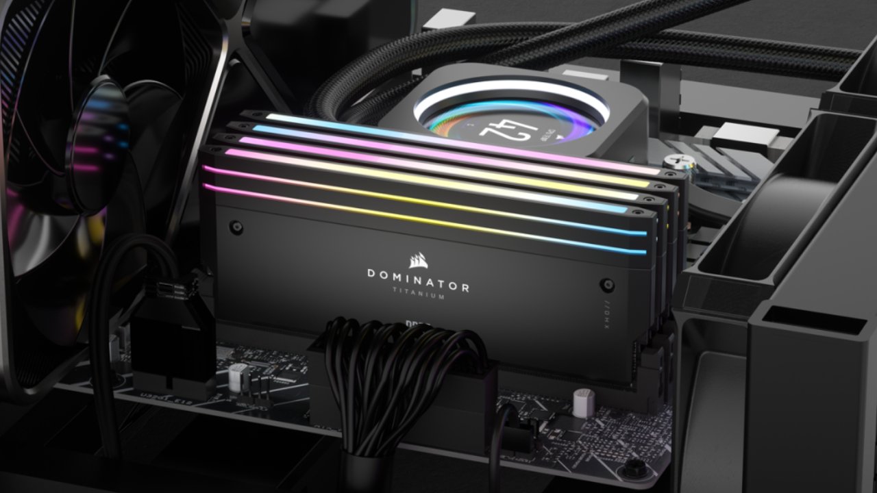
Why Early DDR5 Prototypes Struggle to Boot
Intel Senior Memory Technology Program Manager Gabe Gelfand explained that early DRAM prototypes rarely work on their first boot. The problem comes from developing processors and memory modules simultaneously. CPU makers need working DRAM to test their integrated memory controllers, and memory makers need compatible CPUs to test their latest innovations.
This is a complex chicken-and-egg problem where neither side can wait for the other side to complete development. This is substantially more difficult with DDR5 than it is with DDR4. As transfer rates increase, timing tolerances tighten and electrical operating margins narrow. At the same time, signal integrity becomes more critical, as small differences in voltage, routing, or timing can preclude successful memory initialization.
Another major development is the inclusion of an on-module Power Management IC (PMIC). DDR5 shifts critical voltage regulation duties onto the memory module itself and depends less on motherboard-level power regulation than DDR4. This allows more power-management flexibility, but it also means more variables for engineers to check.
So getting an early prototype to boot up takes more than plugging in the right hardware. You need voltage stability, firmware communication, and memory training to work together.
Inside Intel's Memory Validation Lab
Intel has a comprehensive certification program for thousands of processor-memory combinations to solve these issues. The company partners closely with Samsung, SK hynix, and Micron, as well as JEDEC, to ensure next-gen memory technologies perform reliably across diverse platforms.
That includes voltage behavior, motherboard trace design, memory arrangement, and firmware operation. Engineers must determine whether initialization failures stem from the DRAM, the CPU memory controller, power delivery, or motherboard architecture.
Firmware is especially crucial. Intel MRC (Memory Reference Code) initializes and trains memory, automatically setting electrical parameters and timings to reach a stable operating state. Small adjustments to training methods can mean the difference between a memory configuration that boots successfully and one that fails repeatedly.
That's also why motherboard design is so important to enthusiasts. Varied PCB layouts and memory trace setups can yield substantially different overclocking results, even with the same processors and memory kits.
So, reaching high DDR5 frequencies is more than merely buying pricey modules for overclockers. The outcome depends on the processor's memory controller, the motherboard's topology, the electrical characteristics, and the BIOS implementation.
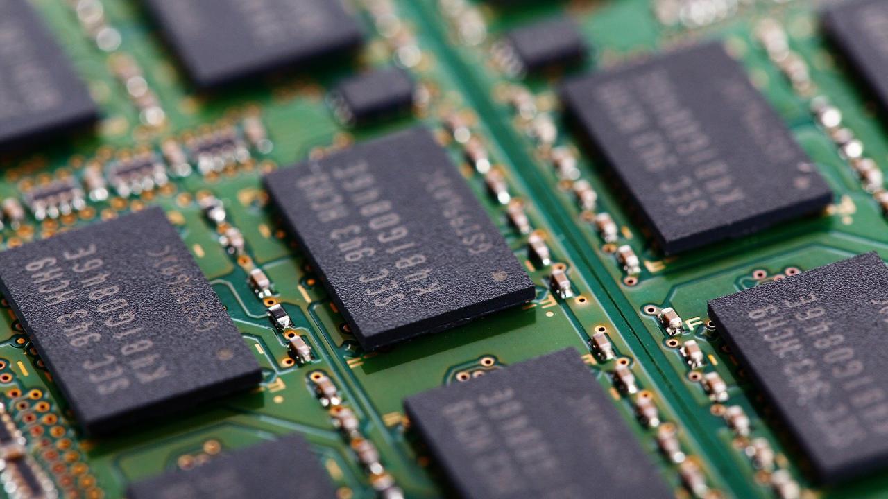
Intel's 256GB CQDIMM Push Could Change Desktop Memory
Intel is also researching CQDIMM (Clocked Quad-Rank DIMM) technology to go beyond classic desktop memory restrictions. Multiple DIMMs per memory channel can limit frequency in traditional setups. Adding more modules also increases the electrical burden on the memory controller, making signal integrity and high-speed operation more difficult.
Conversely, CQDIMMs include a Clock Driver (CKD) directly in the four-rank memory module. This helps regulate clock signal distribution across the module, enabling manufacturers to improve capacity while overcoming the electrical problems of adding memory ranks.
A single module can reach 128GB, meaning two modules can provide 256GB capacity on a motherboard with just two DIMM slots. ASRock has already demonstrated this potential using its Z890I Nova WiFi R2.0 motherboard. The compact Mini-ITX platform successfully operated with two 128GB Kingston CQDIMMs at DDR5-7400 speeds.
The demonstration is particularly interesting because high-capacity memory configurations traditionally require frequency compromises. With 256GB loaded, 7,400MT/s suggests capacity and acceptable bandwidth don't have to compete. But real-world results depend on CPU compatibility, motherboard design, and firmware support.
DRAM Density Keeps Increasing Across Intel Platforms
Intel also reaps the benefits of advances in memory density and Integrated Memory Controllers (IMCs). Alder Lake supported 16Gb DRAM dies (2GB per chip), while Raptor Lake added support for 24Gb dies (3GB per chip). Arrow Lake took this even further with 32Gb dies, or 4GB per chip.
This lets manufacturers create higher-capacity modules without adding more physical memory chips.
FAQ
Q. Why do early DDR5 prototypes frequently fail on their first boot?
A. Early DDR5 prototypes often fail because processors and memory modules are developed simultaneously, creating compatibility challenges involving signal integrity, voltage stability, timing tolerances, and memory training.
Q. What is a CQDIMM, and how does it support 256GB of memory?
A. CQDIMM (Clocked Quad-Rank DIMM) uses an integrated Clock Driver and a four-rank design to support higher memory densities, allowing a single module to reach 128GB and two modules to provide 256GB.
Q. What DDR5 speed did ASRock demonstrate with 256GB of CQDIMM memory?
A. ASRock demonstrated two 128GB Kingston CQDIMMs running at DDR5-7400 on its Z890I Nova WiFi R2.0 Mini-ITX motherboard.
Q. Why is Intel working with Samsung, SK hynix, and Micron on memory validation?
A. Intel collaborates with these memory manufacturers and JEDEC to test processor and DRAM compatibility, improve memory training, and resolve electrical and firmware issues before products reach consumers.
Editor, NoobFeed
Gaming Hardware Updates
No Data.