
Samsung Relies on TSMC 3nm for NVIDIA's Next-Gen NVHBM
Samsung's decision to outsource NVIDIA's custom memory base dies highlights TSMC's growing dominance in advanced semiconductor manufacturing.
Hardware by Masaru Hoshino on Nov 09, 2026
Samsung Electronics is reportedly preparing to use rival TSMC's 3nm manufacturing process to produce the base dies for NVIDIA's next-generation custom high-bandwidth memory, known as NVHBM. For a company that has spent years promoting its integrated memory and foundry capabilities, relying on its biggest manufacturing competitor represents a remarkable departure from its traditional strategy.
The reported arrangement is about more than securing production capacity. It signals that the AI chip business is moving away from traditional foundry rivalry and focusing on manufacturing consistency, sophisticated logic integration, and production yields.
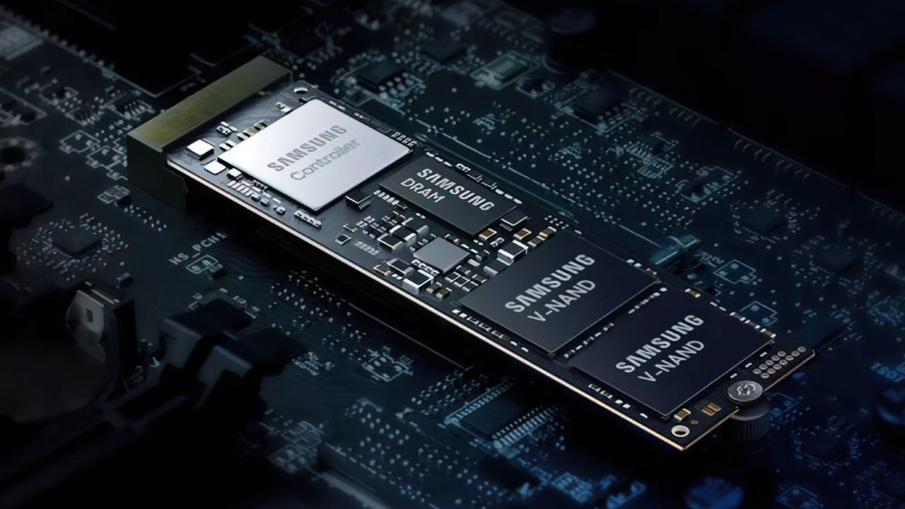
Samsung, SK hynix and Micron are expected to build the base dies of the NVHBM using the same TSMC process, providing the GPU giant more control over memory integration and product validation, sources say. For Samsung, this means accepting that winning NVIDIA's next-generation memory business could require outsourcing a critical manufacturing component to its biggest rival.
NVIDIA Moves Memory Control Into HBM
The biggest development behind NVHBM is its architectural shift. Traditionally, HBM memory controllers are on the primary GPU or XPU computational die, and the memory stack handles data storage and transfers. Sources say the company's next bespoke architecture will put the memory controller right on the HBM base die.
This turns the base die from a standard interface component into a more sophisticated logic device that performs additional memory-control functions. Moving these operations closer to the stacked DRAM may improve communication efficiency, reduce overhead, and simplify integration between memory and processing hardware.
The benefits may extend beyond memory performance. By moving controller circuitry off the main compute die, space is freed for processing resources, which could increase computational density without dramatically increasing the accelerator package size, according to NVIDIA.
The reported performance targets are particularly interesting. NVHBM might provide up to 30% greater memory bandwidth and 15% less power consumption than regular HBM4E. NVIDIA's architecture might also free up about 25% more area on the primary XPU computation chip, leaving more room for processor cores and supporting circuitry.
These modifications make the base die significantly harder to produce. TSMC's 3nm process is an interesting candidate for manufacturing NVIDIA's next-generation architecture, as it will want to integrate a complex memory controller, which demands some advanced logic skills.
The Foundry Reality: Why Yields Matter in Manufacturing
Samsung's move highlights a grim fact about its foundry operations. The business is still a big player in the memory space, but making leading-edge DRAM is a very different game from making leading-edge logic dies.
Samsung's conventional turnkey approach allows it to produce memory core dies and base dies in-house. This gives you more integration and more control over production. But those benefits ring hollow when a large customer asks for manufacturing uniformity that its supplier can't guarantee on its own.
Industry estimates suggest TSMC's 3nm yield is north of 90%, while Samsung Foundry's equivalent SF2 2nm technology is thought to be around 60%. They are estimates, not independently validated production data, and yields are not directly comparable across different nodes and chip designs. But they do show the confidence gap in manufacturing underpinning NVIDIA's alleged decision.
For NVIDIA, irregular yields can translate into increased costs, production delays and issues with product certification. Standardizing the base die manufacturing process across Samsung, SK hynix and Micron reduces those complications.
Crucially, Samsung isn't abandoning its entire turnkey concept. The deal in question is for NVIDIA's bespoke NVHBM specifically. The company will likely continue to produce regular HBM4 and HBM4E products internally and assess its foundry capabilities for future bespoke memory designs.
NVIDIA's Manufacturing Mandate Strengthens TSMC's Position
The arrangement could give NVIDIA unprecedented influence over its memory suppliers. Samsung, SK hynix, and Micron will continue competing through their DRAM technologies, but the underlying logic base die must reportedly follow NVIDIA's preferred manufacturing standard.
This also creates another opportunity for TSMC. If all three major HBM suppliers require its 3nm capacity, TSMC effectively benefits from manufacturing components for companies that otherwise compete against it across the semiconductor industry.
However, increased demand could create another supply-chain bottleneck. TSMC's advanced manufacturing capacity is already heavily contested by smartphone processors, AI accelerators, and high-performance computing products. Producing additional NVHBM base dies could intensify competition for available wafer capacity.
FAQ
Q. Why is Samsung using TSMC's 3nm process for NVIDIA's NVHBM?
A. Samsung is reportedly using TSMC's 3nm process to manufacture NVIDIA's custom NVHBM base dies because NVIDIA wants consistent manufacturing, advanced logic integration, and reliable production yields across all its memory suppliers.
Q. What makes NVIDIA's NVHBM different from standard HBM4E?
A. NVHBM reportedly moves the memory controller from the main GPU or XPU compute die onto the HBM base die, potentially delivering 30% more memory bandwidth, 15% lower power consumption, and 25% more area on the main compute die.
Q. Why does NVIDIA prefer TSMC over Samsung Foundry for 3nm manufacturing?
A. TSMC reportedly offers 3nm yields exceeding 90%, while Samsung's comparable SF2 process is estimated to achieve around 60%. Higher yields can improve production consistency, reduce manufacturing costs, and simplify product validation.
Q. Will Samsung stop manufacturing its own HBM base dies?
A. No. The reported arrangement specifically concerns NVIDIA's custom NVHBM base dies. Samsung is expected to retain its in-house manufacturing strategy for standard HBM4, HBM4E, and other memory products.
Editor, NoobFeed
Gaming Hardware Updates
No Data.