
Intel Nova Lake-H Leak Reveals Six-Tile Design With TSMC N2P and Intel 18A-P
Intel's Nova Lake-H architecture combines six silicon tiles and multiple manufacturing processes to deliver greater flexibility across next-generation laptops.
Hardware by Tanvir Kabbo on Nov 07, 2026
Intel is planning one of its most dramatic architectural overhauls in years with its next Nova Lake-H mobile processors. A fresh leaked die image posted by hardware leaker @momomo_us appears to depict the physical layout of the forthcoming Core Ultra 4000H series, including an exceptionally complex six-tile layout.
More crucially, this design brings together silicon from TSMC and Intel across different process technologies, suggesting how Intel is approaching its next generation of high-performance laptops.
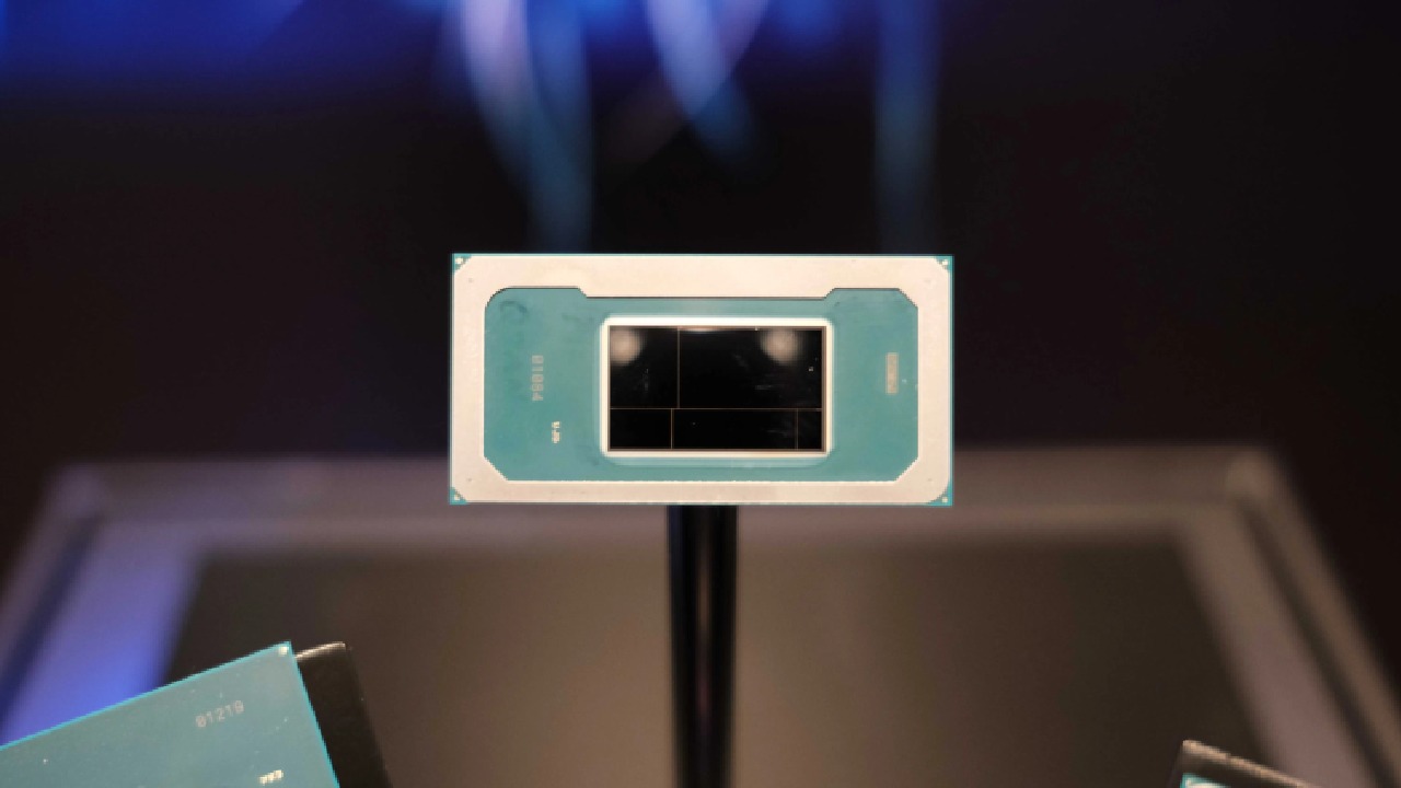
For laptop enthusiasts, it's a fascinating leak, as it gives us a peek at how Intel's disaggregated architecture has evolved. Nova Lake-H moves away from the traditional monolithic design, instead partitioning compute, graphics, and platform functions into distinct tiles. This gives Intel more production flexibility and lets it scale CPUs across multiple laptop types.
Intel Nova Lake-H Introduces a Six-Tile Architecture
The leaked layout shows Nova Lake-H with four active silicon tiles and two passive tiles mostly for structural support. Active components are the Compute Tile, Graphics Tile, Hub/SoC Tile, and Peripheral Controller Tile.
That separation allows Intel to optimize different portions of the chip independently. CPU cores, integrated graphics, and platform connectivity have different performance, power, and manufacturing requirements. Manufacturing them separately could offer more flexibility and possibly reduce the impact of manufacturing faults on expensive silicon.
The two passive tiles offer little computing power, but their presence shows the physical challenge of merging many silicon components into a reasonably compact, transportable container.
Up to 16 CPU Cores Across Two Tiles
The main Compute Tile is said to be ~55 mm² in size and has four Performance cores and eight Efficiency cores. But the overall CPU arrangement goes beyond this tile. Apparently, Intel packed another four Low-Power E-cores onto the Hub/SoC Tile, making Nova Lake-H a 16-core CPU.
That distribution may let the processor handle diverse tasks more efficiently. The Performance cores would handle heavy-duty applications, while the Efficiency and Low-Power cores might handle background activities and lighter duties.
In gaming laptops, this split can help you manage workloads better without unnecessarily firing up the most power-hungry resources. Content creators may also want the extra multicore headroom to run demanding programs alongside background workloads.
TSMC N2P and Intel 18A-P Share Manufacturing Duties
Perhaps the most interesting tidbit is Intel's rumored foundry strategy. The main compute tile is planned to be manufactured using TSMC N2P, while the hub/SoC and peripheral controller tiles are expected to be built using Intel's proprietary 18A-P technology. The Graphics Tile uses a different manufacturing process, with four Xe3 GPU cores made on Intel 3-E.
This mix shows Intel is favoring production flexibility over building each component on a single process node. TSMC's sophisticated N2P technology can optimize the main CPU silicon for performance and efficiency, while Intel makes its other components in-house.
But this approach also creates engineering problems. Different tiles must interact efficiently even when made with different process technologies. With Intel squeezing more components into a single package, power supply, thermal management, and connection efficiency will be especially crucial.
It's also interesting that Intel chose TSMC for its main Compute Tile, given its plans to grow its own foundry. So competitive product performance remains a priority, even if it means relying on an outside manufacturing partner.
Nova Lake-HX Scales Up the Six-Tile Design
Intel's modular architecture could get interesting with the enthusiast-oriented Nova Lake-HX series. The conventional Nova Lake-H package is supposed to be 12 × 23 mm, whereas the HX version is said to be a bigger 12 × 30mm container.
Its Compute Tile is said to be around 104 mm², packed with eight Performance cores and 16 Efficiency cores. This is a huge increase over the regular H arrangement, but it still uses the same six-tile principle.
That scalability could let Intel reuse large chunks of the architecture across the performance spectrum, instead of designing wholly unique CPUs. Gaming laptops and mobile workstations can require a more flexible product portfolio.
FAQ
Q. How many tiles does Intel Nova Lake-H feature?
A. Intel Nova Lake-H reportedly features a six-tile arrangement consisting of four active silicon tiles (Compute, Graphics, Hub/SoC, and Peripheral Controller) and two passive structural tiles.
Q. Which manufacturing processes will Intel Nova Lake-H use?
A. The Compute Tile reportedly uses TSMC's N2P process, while the Hub/SoC and Peripheral Controller tiles use Intel 18A-P. The Graphics Tile reportedly uses Intel 3-E.
Q. How many CPU cores does Intel Nova Lake-H reportedly have?
A. Nova Lake-H reportedly features 16 CPU cores, including four Performance cores, eight Efficiency cores, and four additional Low-Power E-cores.
Q. What is the difference between Nova Lake-H and Nova Lake-HX?
A. Nova Lake-HX reportedly features a larger 104 mm² Compute Tile with eight Performance cores and 16 Efficiency cores, compared to the standard Nova Lake-H's 55 mm² Compute Tile with four Performance cores and eight Efficiency cores.
Senior Editor, NoobFeed
Gaming Hardware Updates
No Data.